

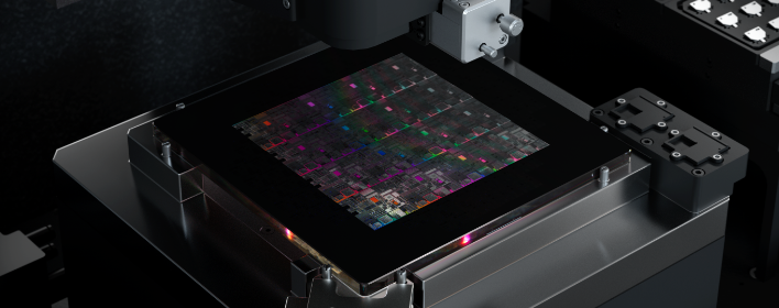
Wafer Processing
Park AFM wafer systems play a crucial role in precise nanoscale measurement and control for wafer fabrication, ensuring accurate construction of devices
Photomask Repair
Park AFM for photomask repair offers a comprehensive solution that streamlines the entire process from automatic defect review to the repair and subsequent verification of the fixes, significantly enhancing repair efficiency and throughput.
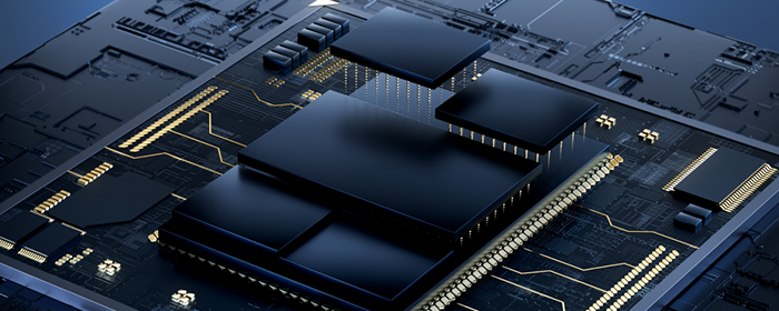
Advanced Packaging
Park AFM's pioneering integration of White Light Interferometry (WLI) enhances quality assurance and process control across all semiconductor manufacturing stages, including advanced packaging and R&D metrology.
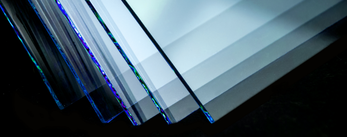
Flat Panel Display
For flat panel display manufacturing, including OLED, LCD, and photonics, Park AFM offers a highly accurate and non-destructive measurement method, optimized for large sample analysis exceeding 300 mm.
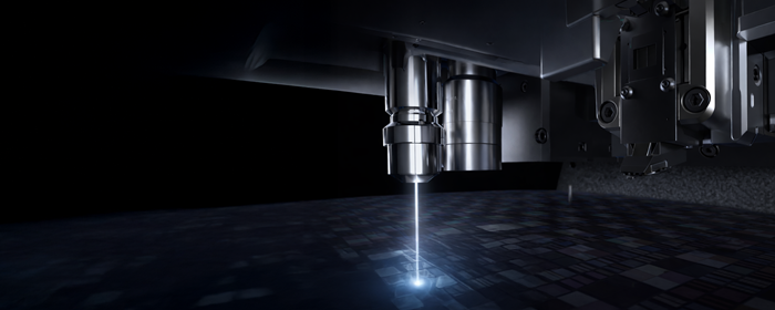
Optical Profilometry
Park Systems’ optical profilometry solutions provide high-speed, non-contact surface metrology with nanometer-level vertical resolution, enabling accurate large-area surface measurement for semiconductor and advanced production environments.

HDD Media Inspection
Park AFM systems enable precise nanoscale surface analysis for HDD heads and automated defect detection for HDD substrates and media, ensuring stringent quality standards and improved manufacturing yield.