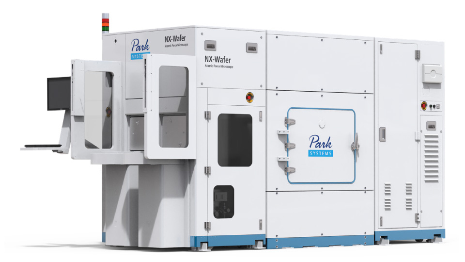
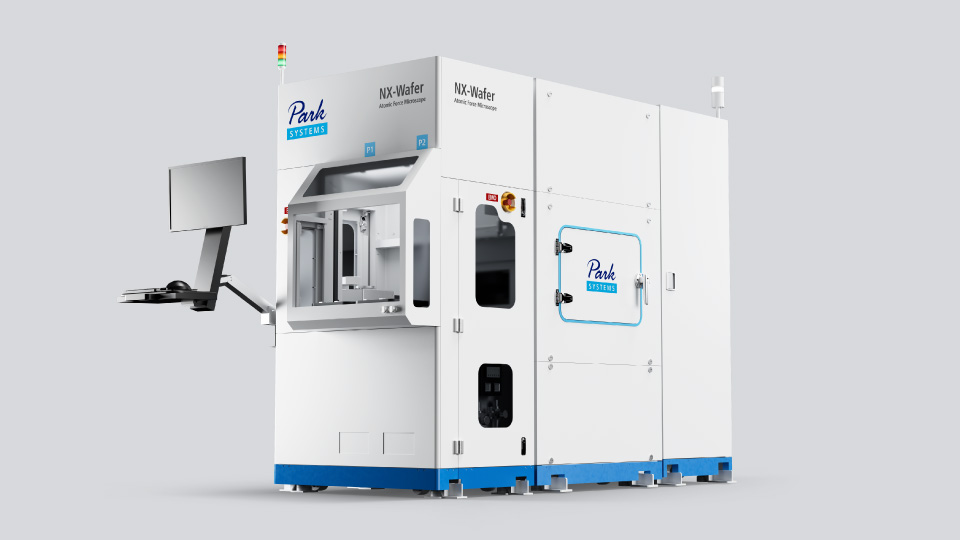
NX-Wafer is an advanced atomic force microscope designed for seamless integration into semiconductor fabrication environments. Leveraging Park Systems’ proven AFM technology, NX-Wafer delivers reliable nanoscale measurement capabilities with full compliance with SEMI standards and complete automation. Widely adopted by major semiconductor manufacturers worldwide, NX-Wafer has established a proven legacy in semiconductor metrology.
Key Features
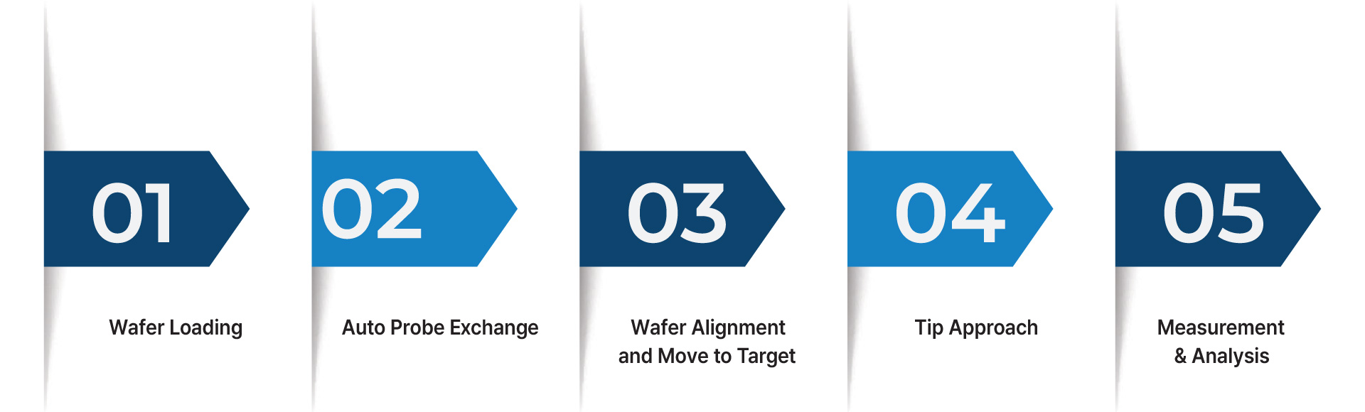
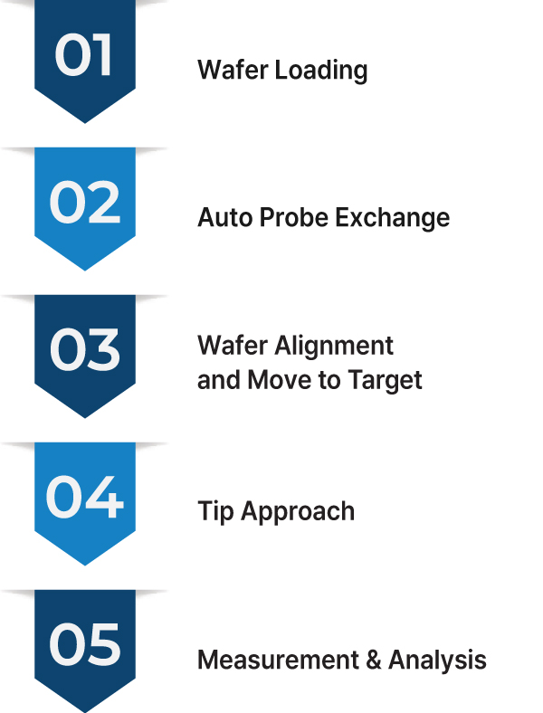
Fully Automated Operation
NX-Wafer enables fully automated operation from wafer handling to measurement and analysis. The system automatically receives recipes from the host and performs end-to-end automation, including selecting the appropriate probe, scanning multiple target areas, analyzing measurement data, and generating reports.
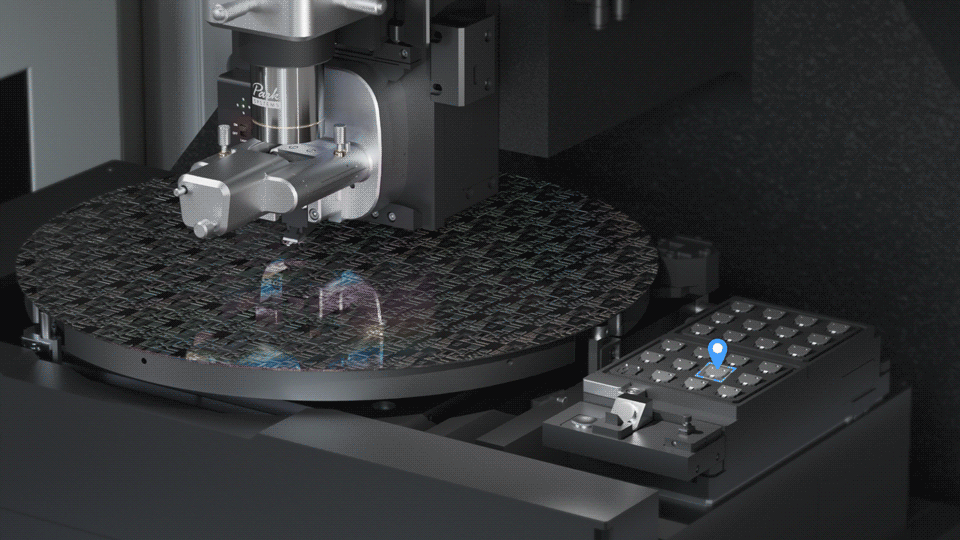
Automated Wafer Handling Capability
Wafer transfer is performed automatically by an equipment front end module (EFEM). It uses robotic mechanisms, sensors, and algorithms to ensure precise alignment and reliable handling of various materials, including warped wafers. The N₂ purge load port is available as an option.
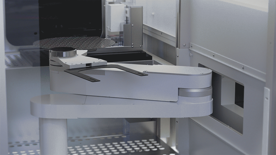
Automatic Probe Exchange
The automatic tip exchanger seamlessly replaces the probe when the threshold is exceeded. It can store up to 24 pre-mounted probes (12 probes per cassette).
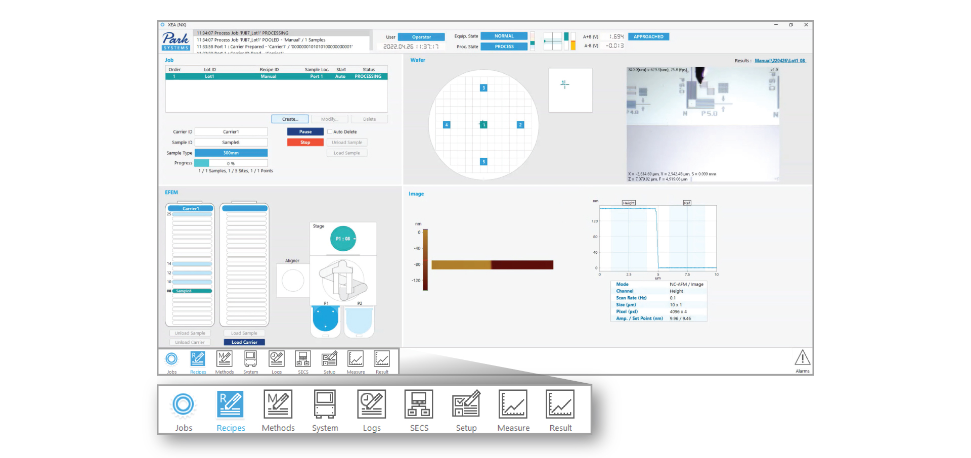
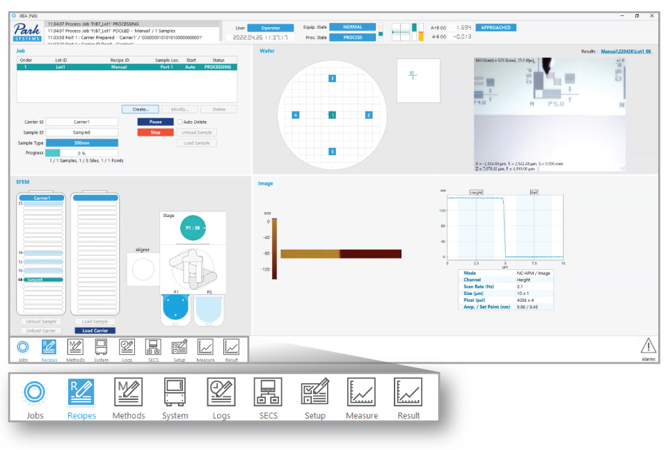
Easy-to-Use Operation Software XEA
XEA offers practical features such as easy copy/paste of recipes, specialized editing modes, and real-time recipe updates. With built-in functions providing comprehensive system operation—including parameter adjustment, database management, and maintenance—the interface remains straightforward and user-friendly. The navigator provides an intuitive user interface that integrates system adjustment and operation.
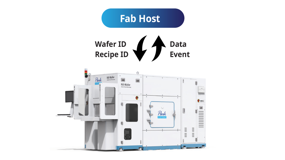
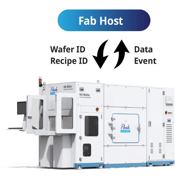
Fab Host Communication via SECS/GEM Protocol
The system enables Fab host communication via the SECS/GEM protocol, ensuring full compliance with SEMI standards including E30, E40, E87, E90, E94, and E84 PI/O for AMHS integration
Fab Compatibility According to SEMI Standards
NX-Wafer ensures optimal compatibility with cleanroom environments in semiconductor fabs. The system achieves ISO Cleanliness Class 1 (≤10 particles/m³ at 0.1 µm and ≤2 particles/m³ at 0.2 µm) and minimizes particle contamination along the wafer movement path through its engineered fan filter unit and ventilation system, while maintaining efficient noise shielding. Additional chemical filters are available as options to effectively block airborne molecular contamination (AMC), which can adversely affect sensitive samples. Furthermore, the system is equipped with advanced monitoring capabilities that can detect and alert users to potential fire hazards or voltage sags.
Park AFM Technology
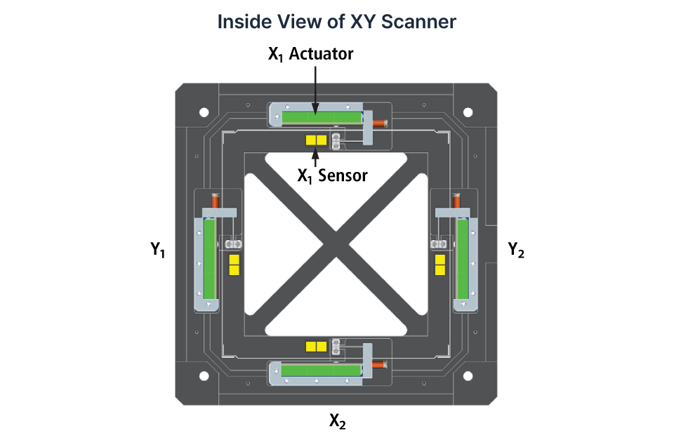
Orthogonal Scan System
The separated flexure-guided 2D XY scanner and 1D Z scanner system minimizes out-of-plane motion by eliminating crosstalk between horizontal and vertical motion. The independent Z scanner enables precise, linear, and fast dynamic performance.
The XY scanner features a dual-servo architecture with two pairs of actuators and position sensors mounted on opposite sides of each axis, providing precise orthogonality and accurate positioning across the entire scan area.
Park AFM Technology
True Non-Contact™ Mode
True Non-contact™ mode, a proprietary technology offered by Park Systems, obtains topography by detecting the attractive van der Waals force between the tip and sample surface. The key advantage of True Non-contact mode is the prevention of tip wear and sample damage, ensuring consistent results with superior data reliability. This also reduces the total cost of ownership by extending tip life. The system also supports contact mode and tapping mode when required.
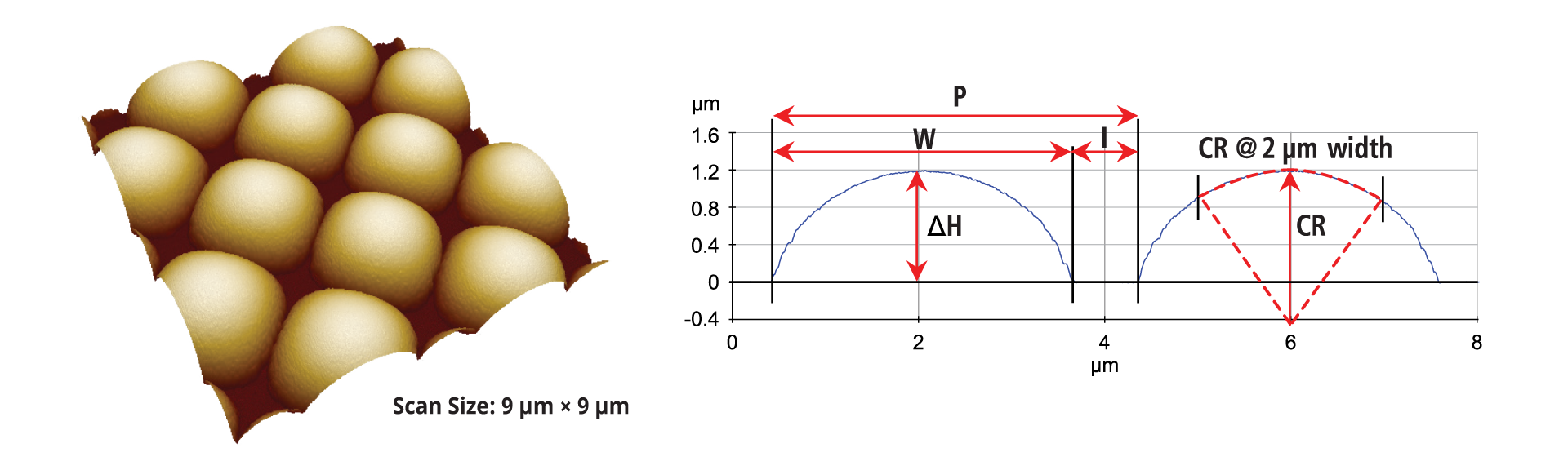
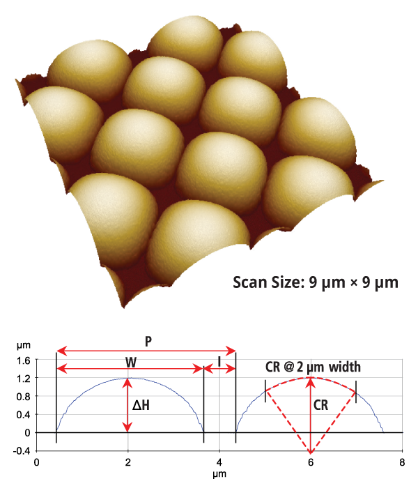
NX-Wafer enables accurate three-dimensional measurement of challenging surface patterns—such as micro-lenses—that are difficult to characterize using optical metrology tools. By providing comprehensive analytical capabilities, including measurements of width, interval, pitch, height, and radius of curvature, it supports reliable nanoscale characterization of complex structures.
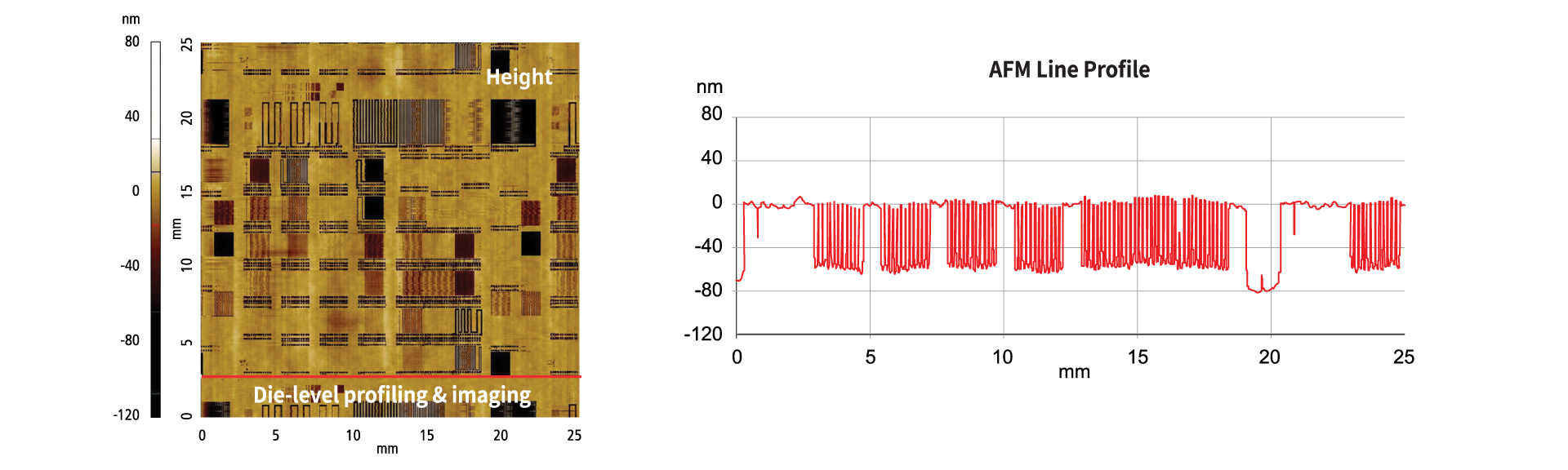
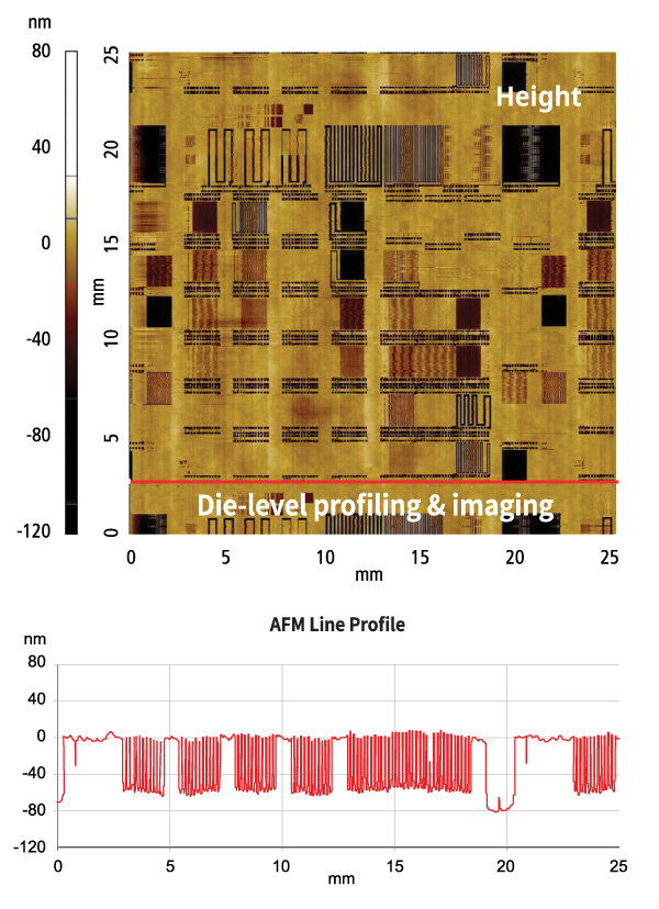
CMP Metrology with Long Range Profiling
By combining NX-Wafer with a sliding stage, the system provides long-range profiling capability for CMP metrology. Park’s automated AFM features a unique sliding stage design that delivers very flat profiling, enabling unprecedented CMP metrology for both local and global planarity measurements, including dishing, erosion, and edge-over-erosion (EOE).
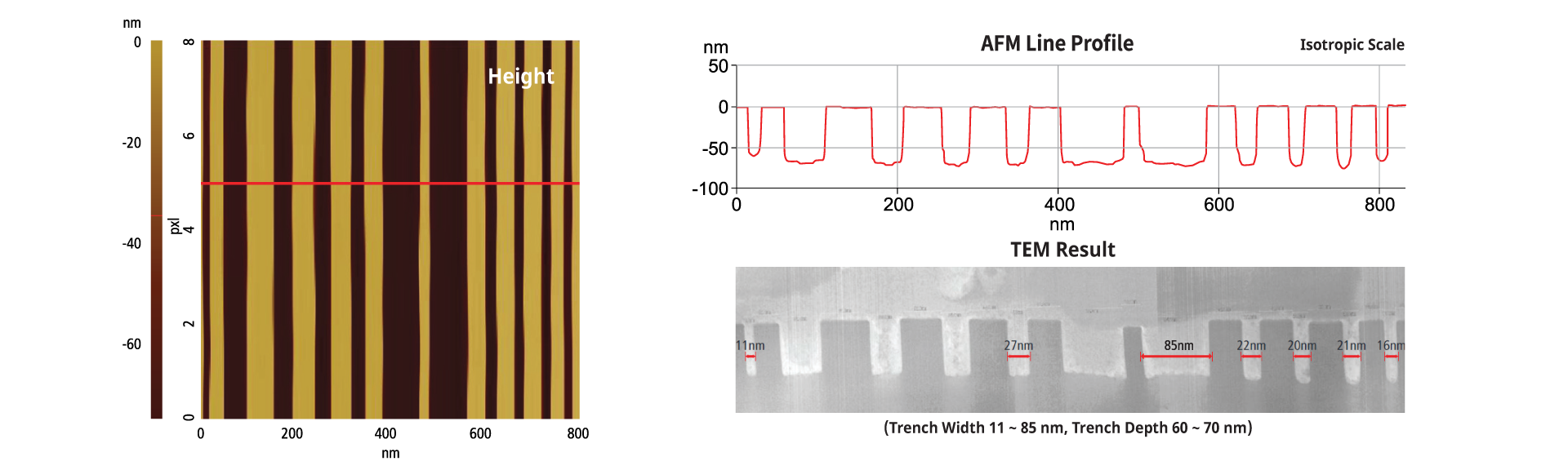
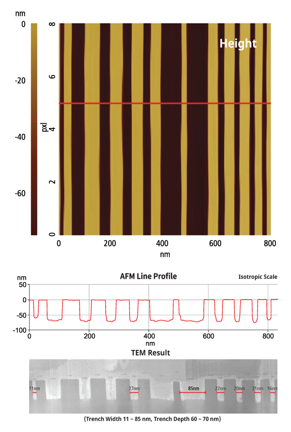
High Aspect Ratio Structure Metrology
Park AFM technology enables measurement of high-aspect-ratio, nanometer-scale trenches used in advanced semiconductor processes. Narrow trench mode (NTM) is optimized for nanometer-scale trench measurements, delivering reliable data for structures with varying aspect ratios. Specialized probes are available to address specific measurement requirements, supporting accurate characterization of challenging trench geometries.
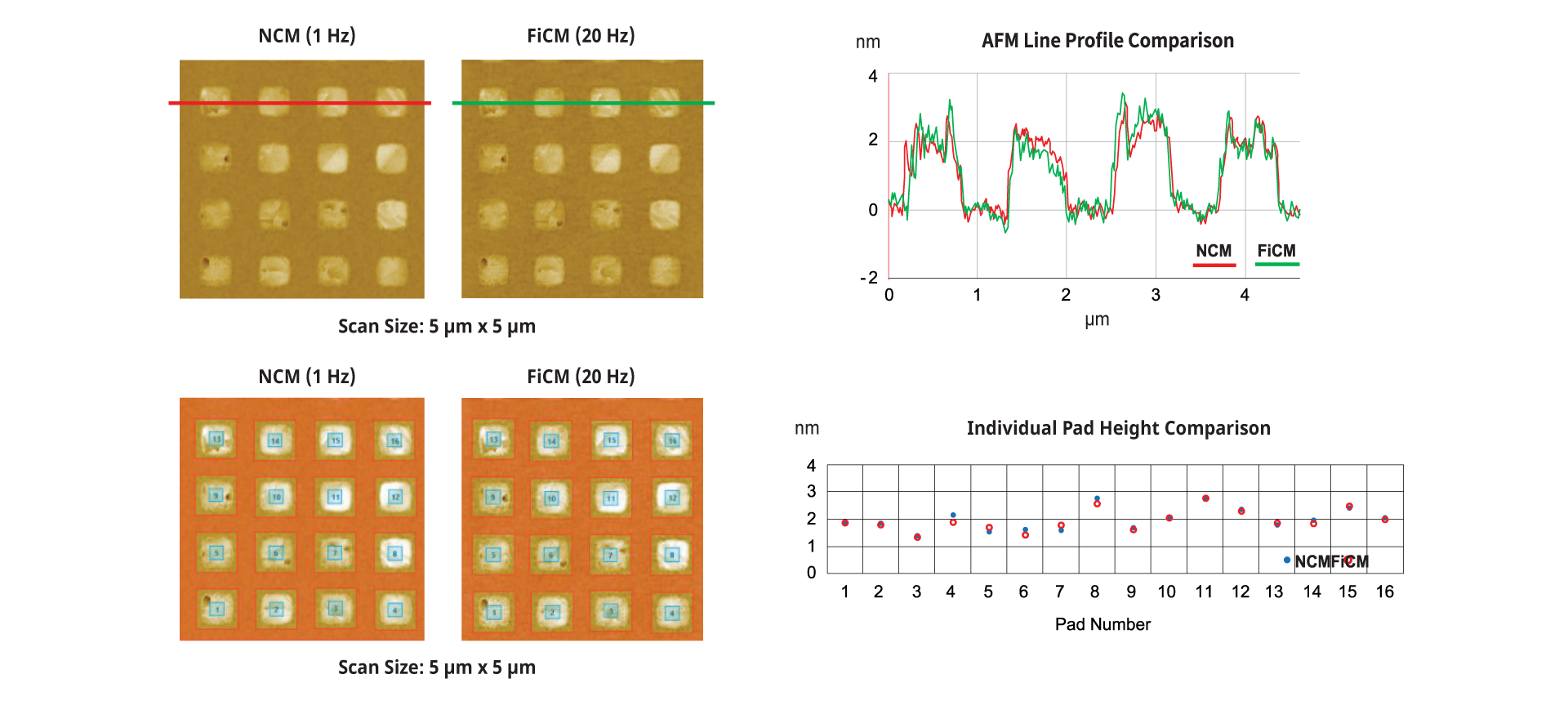
High-Throughput Measurement for Cu Pad
Park’s fast imaging mode (FiM) provides reliable, high-throughput measurement for Cu pad characterization. Cu pad data acquired using fast imaging mode deliver line profiles and height values equivalent to those obtained in True Non-Contact mode, enabling consistent analysis at higher throughput. A proprietary analysis algorithm automatically evaluates each Cu pad regardless of pad shape or array arrangement.
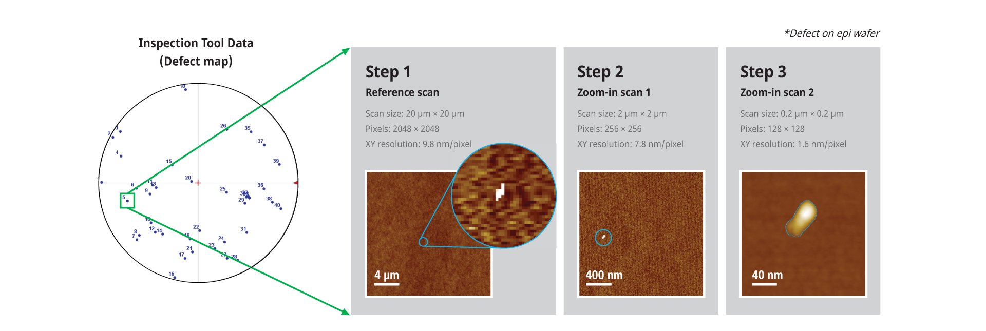
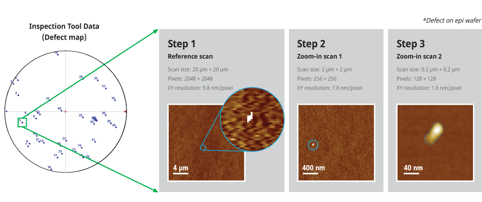
Automatic Defect Review (ADR)
The Automatic Defect Review function enables detailed AFM analysis of defects identified by conventional defect inspection tools. Once inspection data containing defect coordinates is uploaded, the system automatically performs AFM scans at the specified locations. Defect types and surface profiles are then analyzed in detail using zoom-in scan data, supporting consistent and efficient defect
characterization.